AlN (Alminium Nitride)
About AlN
-
AIN (aluminum nitride) single crystal substrate is expected as high efficiency, high frenquency electronical device and deep ultraviolet emitting element.
By using AIN substrate, homoepitaxial growth can be done and defect density of nitride crystal deposition can be controled at a low level.
Now, nitride semiconductor substrate like sapphire, is used as substrate material for ultraviolet emission element. It's obvious that AIN is one of the best substrates from the view of lattice mismatch and ultraviolet light penetrative power.
However it's difficult to produce AIN single crystal substrate from melt liquid since the melt point is high therefore disassociation voltage will be high as well. 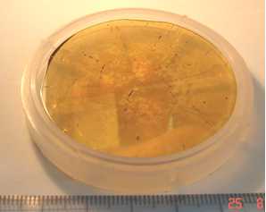
E&M AlN (Alminium Nitride) Wafer's feature
We started handling of bulk Alminium Nitride substrate which is used as advanced materials for R&D of laser(blue to ultraviolet) and power electronic device since 2006.
[Application]
- UV LED/LD, avalanche PD, sensor, power electronic device, heatsink etc.
[Growth]
- Physical Vapor Transport (PVT)
- Sublimation/Seeded-recrystallization of AlN powder
Spec
| Diameter | 22.5~50mm |
| Thickness | 300~700μm |
| Orientation | (0001)±1.0° |
| Finishing | Al face:CMP (RMS <0.8nm) N face:optical (RMS <3nm) |
| Absorbing coefficient | <30cm-1 |
| XRD | FWHM (002):<0.3° FWHM (102):<0.5° |
| EPD | <106cm-2 |
| Effective area | >80% |
| Exclude edge area | 1.0mm |