FZ Wafer
About FZ Wafer
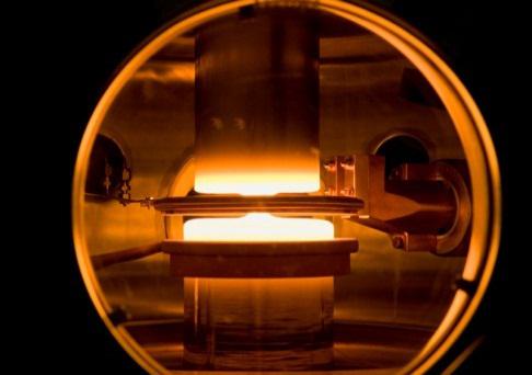
- FZ means floating zone and FZ method is a mono crystal ingot growing method which is different from CZ method.
FZ method is a method wherein seed crystal is attached under multi crystal silicon ingot, and border between seed crystal and multi crystal silicon is melted by induction heat for mono crystallization.
With the characteristics of this method , FZ wafers are wafers of high purity with very low impurity of carbon and oxygen.
Some of them are subjected to neutron irradiation (NTD) in order to control variation of resistivity in radial direction of crystal.
The application of FZ wafers includes MEMS, diode, IGBT, RF device, thyristors(rectifier), high efficiency solar cell and optical products. 
E&M FZ Wafer's feature
We provide NTD wafers radiated by neutron and FZ silicon wafers with low purity doped for power device and solar cells in addition to high frequency IC and MEMS.
We can meet your needs from R&D to mass production.
- Size: ~8inch
