GaP
About GaP
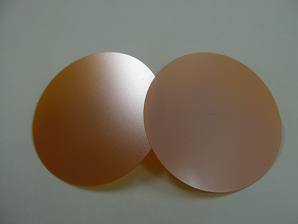
- GaP (Gallium Phosphide) is a orange-yellow semi-translucent material, which is made by direct reaction of galliium and phosphide or reaction by oxide gallium and phosphide at temperature of 900~1000C.
Specific gravity is 4.13,melt point is 1465C, dielectric constant is 9.1,energy range is 2.2eV. GaP has the semiconductor charecteristics as other III-V compounds materials therefore can be used for display elements of various visible light emmition diode as well as illumination (yellow and green) of mobile phone. 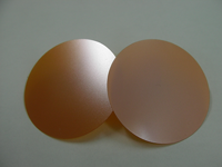
E&M GaP Wafer's feature
- We offer 2inch and 3inch GaP wafer.
【Application】
- Opto device : Visible LED such as display element(red,green) and backlight of LCD(yellow, green) etc.
【Growth】
- Liquid Encapsulated Czochralski (LEC)
Spec
| Type/Dopant | N-type/S,Si,P-type/Zn Un-doped also available |
| Diameter | 2inch ~ 3inch |
| Orientation | (100), (111), (110) Other special orientation or off angle also available. |
| Finishing | Single side mirror polished, Double sides mirror polished, as-cut |
| Thickness | 250-1000um |
| Thickness | (1-10)E18cm-3 |
| EPD | <1E5cm-2 |