Company
Company profile
| Company name | ELECTRONICS AND MATERIALS CORPORATION LIMITED | |
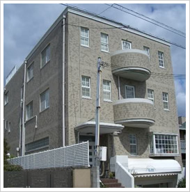
| Location | Head office 11-11, Funado-cho, Ashiya, Hyogo 659-0093 Japan TEL:+81-797-34-6655FAX:+81-797-34-5665 |
|
| Tokyo sales office 1-31-8, Takadanobaba, Shinjuku, Tokyo 169-0075 Japan TEL:+81-3-5291-7070FAX:+81-3-5291-2825 |
||
| Okayama sales office 2nd floor, “Kasaoka Seaside Mall”, 2388, Kasaoka, Okayama 714-0081 Japan TEL:+81-865-62-6688FAX:+81-865-62-6699 |
||
| President | Shinichiro Saito | |
| Foundation | December 2, 1981 | |
| Business | Sales of semiconductor materials,components, machines in Japan and imports/exports for sale. | |
| Capital | JPY25,000,000 | |
| Number of employees | 40 | |
| Shareholders | Kanematsu Corporation(100%) |
|
| Correspondent financial institution | Mizuho Bank/Nada-branch,The bank of Tokyo-Mitsubishi UFJ/Nishinomiya-branch | |
| Main Products | ◇III-V compounds ( GaAs, InP, InAs, InSb etc. ) ◇II-VI compounds ( CdTe, ZnS, ZnTe etc. ) ◇Silicon single crystal wafers ◇Custom III-V compounds and Silicon epitaxial wafers ◇Oxide single crystal wafers ( MgO, STO, LiNbO3, LiTaO3, BGO, Al2O3 etc.) ◇Sputtering targets ( metal, oxide, compounds etc. ) ◇High purity metal elements (Al・As・Ga・In・Sn・Zn etc.) ◇Deposition materials (W. Mo boat type, ITO and the like) ◇High purity carbon jigs ◇MBE related jigs (Mo holder, K-cell gate valve and the like) ◇LED ( chip, lamp, module, advertising display, indirect lighting etc. ) ◇Solar ProductsSolar product ( solar cells, solar panel, solar portable powers ) |
|
History of company
| December, 1981 | Established with capital of JPY 2,500,000 |
| April, 1985 | Increased capital to JPY 10,000,000 |
| July, 1992 | Increased capital to JPY 25,000,000 |
| September, 1996 | Moved to the present address |
| February, 2000 | Established Tokyo sales office |
| August, 2004 | Obtained ISO 14001 certification |
| December, 2005 | Obtained ISO 9001 certification |
| March, 2008 | Established Okayama sales office |
| May, 2025 | 100% subsidiary of Kanematsu Corporation |
Access map
Head office
11-11, Funado-cho, Ashiya, Hyogo 659-0093 Japan
TEL:+81-797-34-6655
FAX:+81-797-34-5665
Transportation Facilities
JR Tokaido Line: five minutes on foot from north exit of "Ashiya" station.
Hankyu Kobe Line: five minutes on foot from north exit of "Ashiyagawa" station.