Customized SOI Wafer
About Customized SOI Wafer
We offer the specification based on customer's requirement.
The following specifications are available.
- 【Device layer】
- Thickness : to thinnest 1.5um
- 【Buried Oxide】
- Buried oxide up to 4um thickness directly
- More than 4um of oxide film are also available
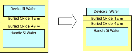
ex) 5um (1um + 4um) Oxide film-Oxide film bonding
- 【Oxide film (more than 4um)】
Buried oxide can be formed by oxide film-oxide film(SiO2+SiO2) bonding (1um + 4um) but this strength is lower than that of silicon-oxide film(Si+SiO2) bonding.
- 【Handle layer】
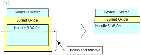
- If you would like handle layer which has less than 300um thickness, we can offer polishing.
- Ex) handle layer : 325um->150um*
- * For thickness,total thickness of SOI wafer shall be measured.
We can process with target tolerance +/-2um.
- 【Backside polish for handle layer】
- We can offer backside polishing for handle layer.
- For thickness,total thickness of SOI wafer shall be measured.
- * Polishing device layer is also available at customer's request.
- 【Field oxide film process】
- We offer field oxide film process on surface of SOI wafer.
- Other films such as nitride film and metal film formation are also available.
- 【Bonding strength】
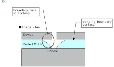
- We can offer SOI wafers which has lower bonding strength between device layer and buried oxide.
- In normal bonding strength, we have past experience that there was no influence on bonding boundary face after etching process for 70 minutes by 48% HF. (based on our past testing data)
- 【Lower bonding strength】
- We can offer SOI wafers which has lower bonding strength.
- 【Standard spec of ICEMOS TECHNOLOGY, LTD.】
- Size: 4inch,5inch,6 inch,8inch
- http://www.icemostech.com/soi-wafers.html