Epi Wafer
About Epi Wafer
-
Epitaxial-growth means the crystal growth being conducted on crystal of substrate and disposed in accordance with foundation of substrate crystal phase.
Homoepitaxial means the growth of the same material as the substrate while heteroepitaxial means the growth of the different material from the substrate. Substrate wafer on which single crystal thin film deposited by epitaxial growth are generally called as epi wafer.
Silicon epi wafers are utilized for element of diode and transistor or substrate for IC such as bipolar type and MOS type.
Furthermore, multiple layer epi wafers and thick film epi wafers are often used for power device and contribute to smallness and energy-saving of various power-source products. 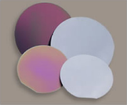
E&M Epi Wafer's feature
Spec
| Thickness | Resistivity | |
| N-type epitaxial Wafer | ||
| Sb,As-doped substrate | to 130μm | 0.01-80ohm |
| P-type epitaxial Wafer | ||
| B-doped substrate | to 130μm | 0.01-80ohm |
| Special epitaxial and multi layer | to 150μm | to 150ohm |