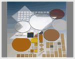
Compound Wafer Products
About WAFER TECHNOLOGY
- We offer high quality products with customer's requirement as the exclusive agent in Japan of Wafer Technology, U.K. based producer.
- Small sized wafers (from 2inch) are available. Please feel free to contact us if you have any requirement.
- WAFER TECHNOLOGY's website:
- http://www.wafertech.co.uk/
Products
III-V Compounds Wafer
GaAs
- E&M GaAsWafer's feature
According to customer's required specification,we can meet your needs in a variety areas from small volume for R&D to mass production.
Besides,special orientation products like (111),(110) and (311) are also available.
| Growth | VGF |
| Type/Dopant | N-type/Si・Te, P-type/Zn, Semi-Insulating/Un-doped |
| Diameter | 2inch ~ 3inch |
| Orientation | (100)・(110)・(111)~(611)For other orientation and off-orientation,please ask us. |
| Finish | Single side mirror polished, Double sides mirror polished, Epi-ready For other treatment,please ask us. |
| Thickness | 2inch: 350or500um, 3inch: 625um For other treatment,please ask us. |
| Others | For career concentration, resistivity, mobility, it can be specified within the allowable range. |
InP
- E&M InPWafer's feature
According to customer's required specification,we can meet your needs in a variety areas from small volume for R&D to mass production.
Besides,special orientation products like (111),(110) and (311) are also available.
| Growth | LEC |
| Type/Dopant | N-type/S・Sn・Un-doped, P-type/Zn, Semi-Insulating/Fe |
| Diameter | 2inch |
| Orientation | (100)・(110)・(111)~(611) For other orientation and off-orientation,please ask us. |
| Finish | Single side mirror polished, Double sides mirror polished, Epi-ready For other treatment,please ask us. |
| Thickness | 2inch: 350or500um, For other thickness,please ask us. |
| Others | For career concentration, resistivity, mobility, it can be specified within the allowable range. |
GaSb
- E&M GaSbWafer's feature
According to customer's required specification,we can meet your needs in a variety areas from small volume for R&D to mass production.
Besides,special orientation products like (111),(110) and (311) are also available.
| Growth | LEC |
| Type/Dopant | N-type/Te, P-type/Un-doped, Zn |
| Diameter | 2inch ~ 4inch |
| Orientation | (100)・(110)・(111)~(611) For other orientation and off-orientation,please ask us. |
| Finish | Single side mirror polished, Double sides mirror polished, Epi-ready For other treatment,please ask us. |
| Thickness | 2inch: 500um, 3inch: 625um, 4inch:1000um For other thickness,please ask us. |
| Others | For career concentration, resistivity, mobility, it can be specified within the allowable range. |
InAs
- E&M InAsWafer's feature
According to customer's required specification,we can meet your needs in a variety areas from small volume for R&D to mass production.
Besides,special orientation products like (111),(110) and (311) are also available.
| Growth | LEC |
| Type/Dopant | N-type/S, Un-doped, P-type/Zn |
| Diameter | 2inch ~ 3inch |
| Orientation | (100)・(110)・(111)~(611) For other orientation and off-orientation,please ask us. |
| Finish | Single side mirror polished, Double sides mirror polished, Epi-ready For other treatment,please ask us. |
| Thickness | 2inch: 500um, 3inch: 625um For other thickness,please ask us. |
| Others | For career concentration, resistivity, mobility, it can be specified within the allowable range. |
InSb
- E&M InSbWafer's feature
According to customer's required specification,we can meet your needs in a variety areas from small volume for R&D to mass production.
Besides,special orientation products like (111),(110) and (311) are also available.
| Growth | CZ |
| Type/Dopant | N-type/Te,Un-doped, P-type/Ge |
| Diameter | 2inch ~ 4inch |
| Orientation | (100)・(110)・(111)~(611) For other orientation and off-orientation,please ask us. |
| Finish | Single side mirror polished, Double sides mirror polished, Epi-ready For other treatment,please ask us. |
| Thickness | 2inch :625um, 3inch :800/900um, 4inch :1000um For other thickness,please ask us. |
| Others | For career concentration, resistivity, mobility, it can be specified within the allowable range. |
Other Compound Wafer
AlN
- E&M AlN (Alminium Nitride)Wafer's feature
We started handling of bulk Alminium Nitride substrate which is used as advanced materials for R&D of laser(blue to ultraviolet) and power electronic device since 2006.
- 【Application】
- UV LED/LD, avalanche PD, sensor, power electronic device, heatsink etc.
- 【Growth】
- Physical Vapor Transport (PVT)
- Sublimation/Seeded-recrystallization of AlN powder
- 【Spec】
| Diameter | 22.5~50mm |
| Thickness | 500±50um |
| Orientation | (0001)±1.0° |
| Finish | Al face:CMP (RMS <0.8nm) N face:optical (RMS <3nm) |
| Absorbing coefficient | <30cm-1 |
| XRD | FWHM (002):<0.3° FWHM (102):<0.5° |
| EPD | <106cm-2 |
| Effective area | >80% |
| Exclude edge area | 1.0mm |
GaP
- E&M GaP Wafer's feature
- We offer 2inch and 3inch GaP wafer.
- 【Application】
- Opto device : Visible LED such as display element(red,green) and backlight of LCD(yellow, green) etc.
- 【Growth】
- Liquid Encapsulated Czochralski (LEC)
- 【Spec】
| Type/Dopant | N-type/S,Si,P-type/Zn |
| Diameter | 2inch ~ 3inch |
| Orientation | (100), (111), (110) Other special orientation or off angle also available. |
| Finish | Single side mirror polished, Double sides mirror polished, as-cut |
| Thickness | 250-1000um |
| Thickness | (1-10)E18cm-3 |
| EPD | <1E5cm-2 |
- 【Others】
- ※For more details,please Contact Us.
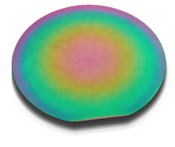
Al2O3(Sapphire)
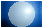
- E&M Al2O3Wafer's feature
Sapphire is a material which has good crystal characteristics and low-dielectric constant We can offer 2”,3”,4” epi-ready substrate and custom requirements such as off-orientation,both sides polished,thickness etc are also acceptable.
- 【Application】
- LED, Substrate for GaN
- 【Spec】
| Diameter | 2inch ~ 4inch |
| Orientation | C(0001)0.2off±0.1°to m-axis |
| OF direction | (11-20)±0.3° |
| OF length | 2inch:16±0.5mm, 4inch:30±1.0mm |
| Thickness | 2inch:430um, 4inch:650um |
| Finish | One side epi polished |
| Bow | ≦10um (2inch) |
| TTV | ≦10um (2inch) |
II-VI Compounds Wafer、Others, Special Specification
- 【Product】
CdSe
CdS
ZnSe
ZnTe
ZnS
SiC
- E&M SiCWafer's feature
We supply SiC wafer from 2inch" to 4inch" for vatious applications.
*SiC epi wafer is also available.
GaN
- E&M GaNWafer's feature
We supply high quality GaN bulk substrate for LED,LD and device applications.
- Size:~2inch"
*GaN Epi wafer is also available
Ge
- E&M GeWafer's feature
We supply 2inch~4inchGermanium wafer for applications such like infrared,solar cell and detector.
Oxide
- E&M OxideWafer's feature
We supply various oxide single crystal wafer such like
- MgO,SrTiO3 and ZnO etc.
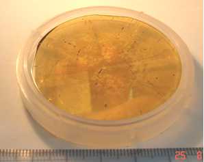
Epi Wafer
Compound Epi Wafer
- E&M Compound Epi Wafer's feature
We supply various compound epitaxial wafers.
<Electronical device application>
- HBT, pHEMT, BiFET, BiHEMT etc
- VCSEL, LD, PIN, APD, LED and multi-joint solar cell etc.
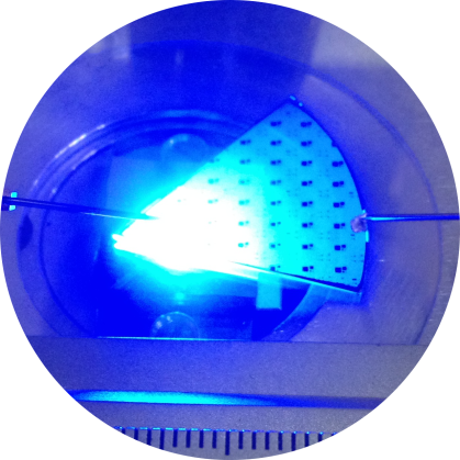
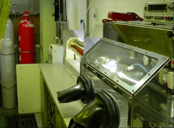
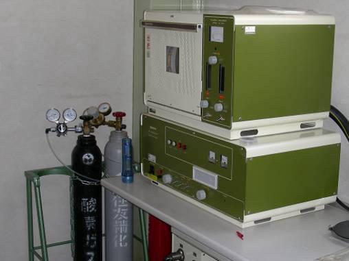
LPE growth processing
Compound semiconductor processing service
-
E&M makes every endeavor to meet the needs from R&D Dept for fundamental experiment, trial production within a short leadtime, or problem check before formal trial experiment.To achieve this goal we have installed the equipment and developed technology for "anything-goes" on our own investment.
We can offer LPE growth with design and manufacture of exclusive crystal growth boat to maximum 2inch. Process equipments are Sputter, Contact Aligner and Plusma Etcher.Please see below our available process and specification.Please contact us for R&D and trail production.