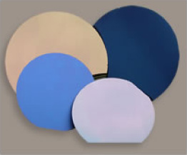
Film Wafer
About Film Wafer
- Wafers processed with film deposition is called film wafer.
Examples of film to be used (growth of film) include isolation film as isolation material between layers, metal film as conductive material, process material such as resist and protective film.
The main methods are thermal oxidation method, CVD method (Chemical Vapor Deposition), and PVD method (Physical Vapor Deposition).
A thermal-oxidized film(SiO2)is formed on both sides of wafer for film forming process in diffusion furnace. On the other hand, in plasma CVD and sputtering (PVD) method, a film is deposited on one side of wafer due to process per single wafer.
As mentioned above, film wafers have different characteristics due to different methods and are used for different purposes according to film type. 
E&M Film Wafer's feature
We offer film formation service such as metal film and thermally-oxidized film etc.
- Size: 2inch ~ 12inch
- thermally-oxidized film, Si3N4 film, TEOS, BPSG, Cu film, Al film, Ti film, Ta film, TaN film, TiN film etc.
- For photolithography process, we can produce mask with customer's requirement and also offer patterning process with standard mask as well.
